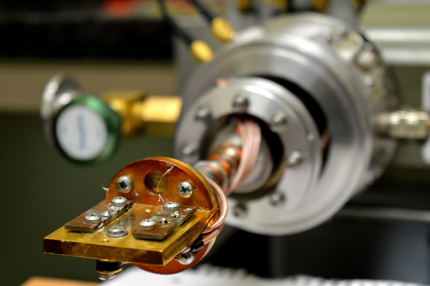
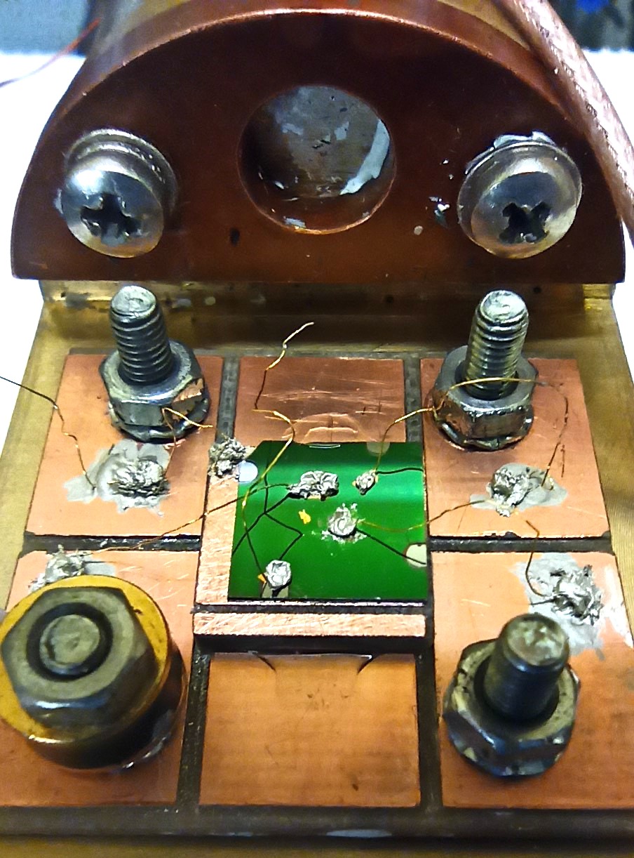
A tool for investigation active defects (traps) in semiconductors. It gives insigth into defect parameters: activation energy and capture cross-section. Our DLS-82E system operating within 77-300 K temperature range consists of:
and gives us an opportunity for Laplace DLTS technique.
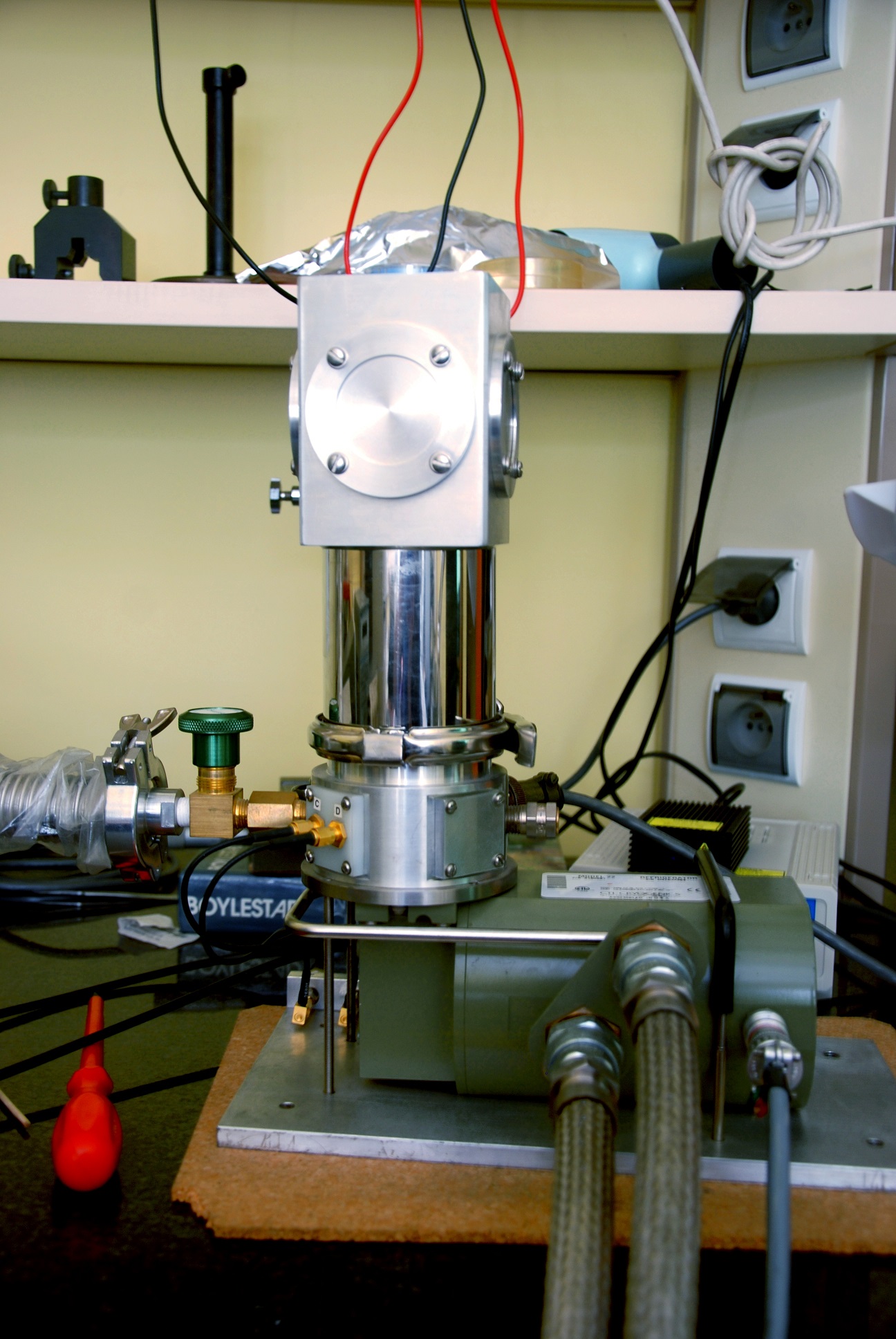
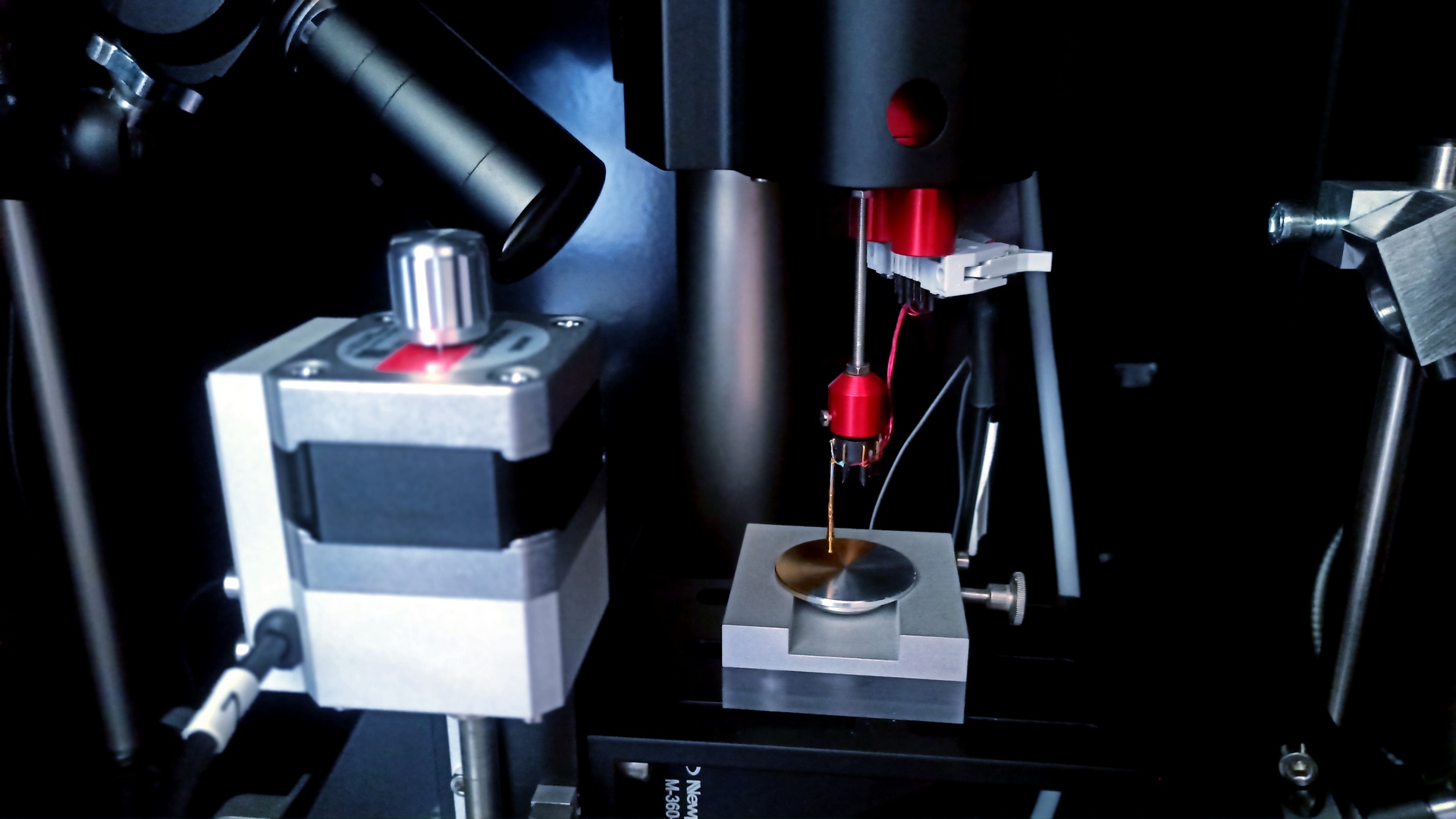
The aforementioned staff enables electrical measurements of temperature range of 10-350 K and establishing fundamental parameters of p-n junction:
The photovoltaic parameters can be investigated in the LEPS as well with the I-V curve tracer and SS100AAA - 500 Watt Solar Simulator.
The other photovoltaic measurements are ensured by PV3000 Quantum efficency system Betham:
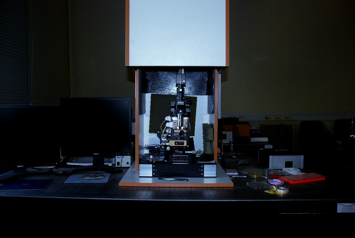
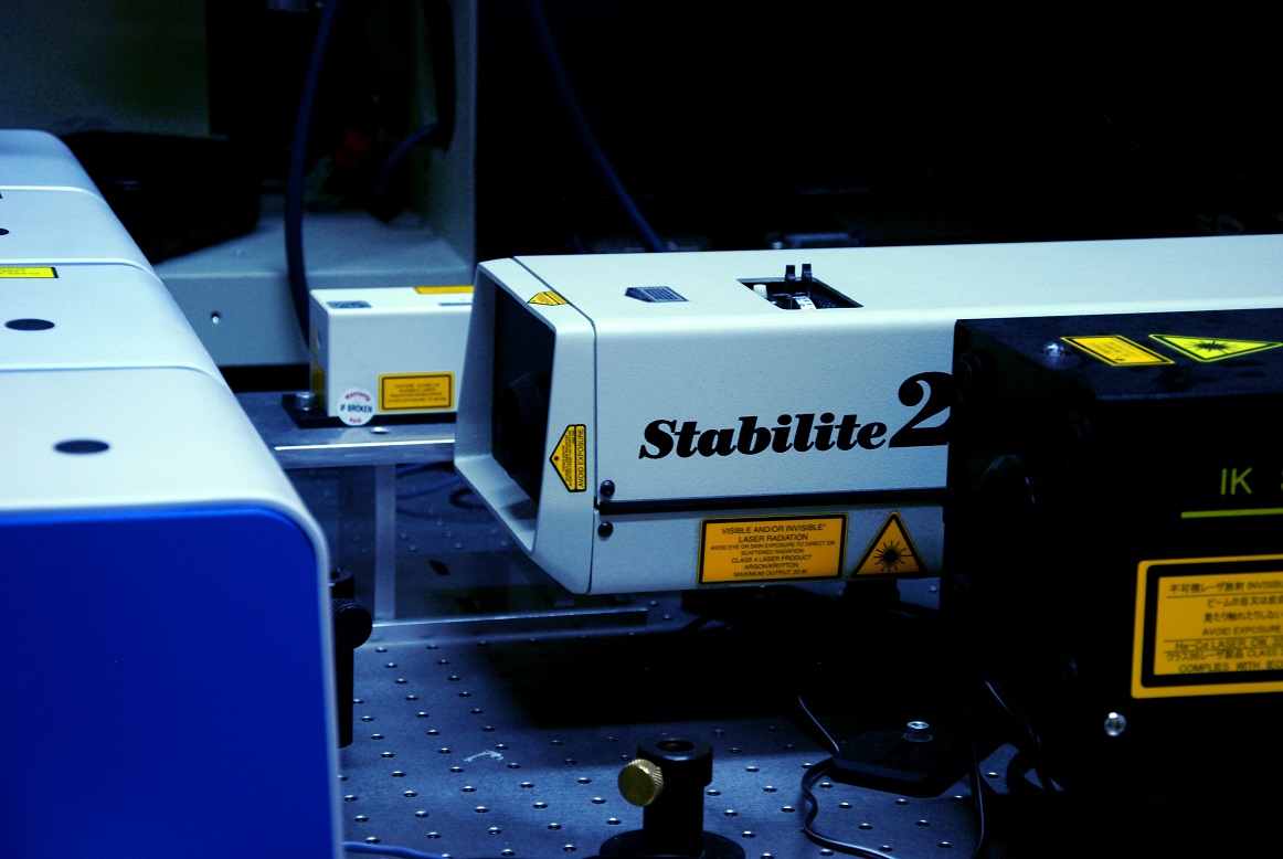
Our setup for photoluminescence measurements includes:
and is adapted for broad temperature range of 10 - 350 K.
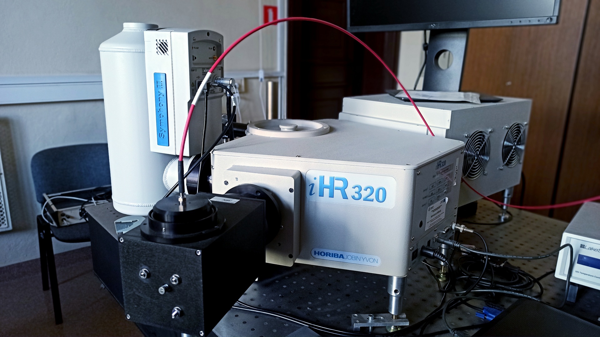
For the investigation of phonon spectra the high resolution (~0.5cm-1) T64000 Horiba-Jobin-Yvon Raman spectrometer is used.
created with
HTML Designer .